FPGA has emerged as a versatile and powerful technology with a rapid prototyping platform for designing complex and efficient digital electronic solutions. It’s an ideal tool not only for learning digital circuits and systems but is also the best solution for hardware prototyping and verification of digital designs – FPGA does not require the high non-recurring engineering (NRE) costs associated with custom ASIC (Application Specific Integrated Circuits) designs. Since FPGAs can be reconfigured, they are suitable for a wide range of applications in consumer, automotive, telecommunications, networking, aerospace, and other industries. FPGAs are also used for DSP tasks (audio and image processing and software-defined radio).
As the need for machine learning devices grows worldwide, many major market players invest in high-speed computing processors. While AI is primarily based on software algorithms that mimic human thinking, custom hardware is becoming an increasingly important component. FPGAs and Graphics Processing Units (GPUs) are the two main hardware solutions for most AI operations. Some examples of FPGA-based machine learning and AI projects include:
- Deep learning accelerators
- AI processing at the edge
- Implementation of custom AI algorithms for optimizing performance and power efficiency
FPGAs offer high performance, easy (re)configuration and parallelism but can be more expensive and power-hungry compared to ASICs, PLDs (Programmable Logic Devices), and microcontrollers when high-volume production is required. They are cost-effective for low-volume production and well-suited for proof-of-concept projects allowing engineers to study designs before they are built commercially.
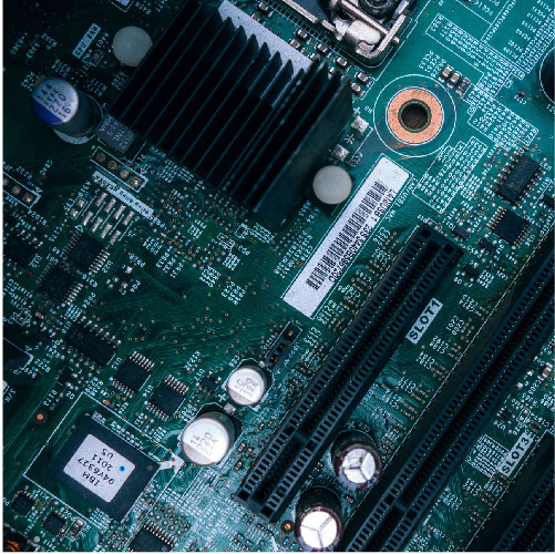
Internal Structure of FPGA
Each FPGA vendor has its own FPGA architecture. Still, in general terms, they are all variations of what is given in Fig.1. Each FPGA fabric contains a matrix of configurable (programmable) logic blocks connected via configurable interconnects.

Configurable Logic Blocks (CLBs) are the basic building blocks of an FPGA. They contain RAM for creating arbitrary combinational logic functions, also known as lookup tables (LUTs), flip-flops, multiplexers for routing the logic within the block or to and from external resources, and sometimes dedicated arithmetic units. CLBs can be configured to perform various combinational and sequential logic functions. These CLBs contain enough logic to create a small state machine.
Programmable Interconnect Points (PIPs) or switching matrices are the programmable switches and wiring resources that connect CLBs and other components within the FPGA. PIPs allow flexible routing and interconnection of signals between different elements on the chip.
Input/Output Blocks (IOBs) are the interface points through which data transfers between the FPGA and external devices or other components on the board. IOBs are configurable to support various signaling standards and protocols, enabling the FPGA to communicate with a wide range of peripherals.
Modern FPGAs also contain components specialized for specific functions, such as:
- Block RAM (BRAM)
- DSP blocks
- DSP slices
- Clock management resources (PLLs and DCMs)
- Configuration memory
Further, the FPGA’s can contain Hard IPs (e.g. Ethernet, DDR I/F, and one or more CPUs often referred to as SoC System on a Chip).
Hardware Description Languages
The FPGA configuration is generally specified using Hardware Description Languages (HDLs). With HDL, engineers describe hardware behavior and their structure in textual form. But HDL is not a software programming language, but a description syntax. Traditional software programming language is translated into machine instructions and executed on a computer. As a distinction the as the name implies, HDL is a language with syntactic and semantic support for modeling hardware’s temporal behavior and spatial structure. HDL description of a digital circuit is implemented directly into the hardware using an FPGA. So, writing an efficient HDL code requires a deeper understanding of digital circuit design and FPGA resources.

HDLs are used to describe digital circuits at a high level of abstraction. The two primary HDLs used in FPGA design are VHDL and Verilog. VHDL (VHSIC- Very High Speed Integrated Circuits Hardware Description Language) is ADA-like verbose language that provides a high level of abstraction, making it easier to write complex designs. Verilog has a C-like concise syntax. It has a lower level of abstraction compared to VHDL, which can make it more challenging for complex designs but also allows for greater control over the design. The choice between these two HDLs often depends on personal preference or industry standards.
To get started with FPGA design, one needs an HDL editor, simulation tools (e.g., ModelSim, XSIM, synthesis tool (e.g., AMD Vivado, Intel Quartus. Lattice Diamond), and implementation tools (e.g., AMD Vivado, Intel Quartus, Lattice Diamond). Based on the application requirement, three types of FPGAs can be selected:
- low-end
- mid-range
- high-end
ECP3 and ECP5 series from Lattice semiconductor, Artix-7/Kintex-7 series from Xilinx, and Stratix family from Intel are some of the popular FPGAs for low power and low design density.
Unlock the full potential of your projects with our cutting-edge FPGA services!
Whether you’re in need of high-performance computing solutions, customized designs, or seamless integration, our expert team is here to turn your vision into reality. Don’t settle for less – experience the power, flexibility, and innovation that only our FPGAs can deliver. Let’s get in touch today and start your journey towards unparalleled performance and efficiency!